The time resolution of the TOF system is designed to be less than 80 ps, which corresponds to pi/K separation up to momentum of 2.4 GeV/c at the flight path of 5 m. Since the TOF counters have the intrinsic timing resolution less than 80 ps, which was checked at KEK in 1995, the TOF FEE system should have better timing resolution than 25 ps. "Near deadtimeless operation" means that the TOF FEE system is not completely deadtimeless since the PHENIX has 4 beam crossing dead time after each LVL-1 trigger. To fulfill requirement of the data storage, we have adopted the switched capacitor analog memory unit with 64 cells deep. The switched capacitor array approach to pipelining analog TOF counter signals offers high density, fast sampling speeds, wide dynamic range, and a high degree of flexibility.
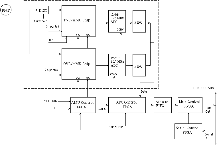
Figure 1: FEE block diagram. TOF FEM block diagram showing data stream. Each TVC/AMU chip and QVC/AMU chip have 4 input channels and 4 of each chip are mounted on an FEM board (16 channels/FEM).
When a particle created by nuclear collision hits a scintillator slat attached to two PMTs and light guides on both ends, the anode pulses from the PMTs are observed. The anode current is fed to a leading edge discriminator. The logical true of the discriminator output is asserted when the analog signal crosses the threshold which is set via serial control in the board initialization stage. The output signal from the discriminator is sent to the Time-to-Voltage Converter (TVC) and Analog Memory Unit (AMU) chip (NEVPHX05) which is shown in Figure 2, to start the TVC.

Figure 2: TVC/AMU chip (NEVPHX05) block diagram.
The next beam clock stops the TVC from charging further. The voltage induced by integrated constant current in the TVC is sampled at the RHIC beam crossing frequency, and stored in the AMU which consists of long 64-cell switched capacitor array until a LVL-1 trigger decision is made. The TVC is reset two beam clock later, making it then ready for a new hit. Thus TVC takes three beam clock cycles to be ready for the next measurement. The other split analog signal is sent to the Charge-to-Voltage Converter (QVC) and AMU chip (NEVPHX06). The QVC measures the integrated charge information from the PMT. The net charge found on the anode is determined by comparing two samples from the AMU; a pre-sample stored just before the event and a post-sample stored just after the event. The QVC is reset periodically to discharge the integrator since the QVC integrator is a continuously charge integrator. When the LVL-1 trigger signal is received by the on-board AMU control Field Programmable Gate Array (FPGA), the TVC and QVC values stored in an AMU cell are transferred for digitization by a 12-bit 1.25 MHz ADC. The timing chart of the TOF FEE system is shown in Figure 3.

Figure 3: TOF FEE timing diagram. Note that we use the system clock timing of 112 ns instead of 106 ns.
Operations of the AMU and the ADC are controlled by on-board AMU control FPGA and ADC control FPGA, respectively. The AMU controller specifies the Write Addresses (WA) and the Read Addresses (RA) for specific AMU cell. It also serves as a multiplexer for the four channels in TVC/QVC chips to corresponding ADC. The AMU controller manipulates the AMU cell addresses to accommodate the requirement for simultaneous read and write requirement into these memories. The ADC controller generates the convert (CONV) signal for the digital conversion, and also takes care of the data formatting. These FPGAs also provide the interface to the LVL-1 trigger, and adds event header in the data stream , namely, event number, FEM address, AMU cell address and FEE link status into a 512-words x 18-bits FIFO (First In First Out) memory which becomes part of the event record. The Link controller is responsible for handling the token transfer operation between the FEE control card and the FEM.

Figure 4: A picture of the Front-end Electronics Module.

Figure 5: Analog Memory Unit block diagram.
The Read and Write switches are controlled independently by separate buses. Thus, while one sample is being read out, it is possible to continue to sample the input voltage and write the samples to other cells in the same pipeline. In order to enable random access to any pipeline cell both for Write and Read operations, the AMU controller needs to provide Write and Read address correctly. The AMU controller does the address bookkeeping in a series of FIFOs in an AMU controller. The FIFO in the on-board AMU controller contains the list of AMU cells which are available to be written, and are associated with a LVL-1 trigger and are awaiting digitization. Once the data corresponding to a AMU cell has been digitized, the address is written to a FIFO which contains those addresses which can be reset as being available to be written. The logic governing the operations of the FIFOs is set up to always choose as the next WA the first available cell found by incrementing past the current AMU cell. In this way, the sequence of WA's is kept as numerically ordered as possible.

Figure 6.1: Bench test setup of the TOF FEE system at Nevis Lab. Columbia Univ. We developed a test pulse generator which can be generate accurate system clock timing of 112 ns and test pulse with 3.5 ns step which is synchronized with the system clock timing. The timing difference between test pulse and system clock timing can be used as the timing calibrator for the TVC.

Figure 6.2: Bench test setup of the TOF FEE system at Nevis Lab. Columbia Univ.

Figure 7: TVC timing test using test pulse with 3.5 nsec step. The top figure shows measured TVC distribution. The bottom figure shows timing of the test pulse vs TVC values. This shows excellent integrated linearity over the whole range of the TVC (4096 channels).


Figure 8: Left: TVC time constant [psec/channel] distribution for each TVC channel extracted from the bottom plot of Figure 7. The average value is 28.0 [psec/channel]. Right: AMU cell dependence of the TVC time constant. The error bar shows statistical error only. The cell dependence was not seen within statistical error of 0.8%.

Figure 9: TVC distribution with random timing pulse. The TVC value is separated from the pedestal around 3950 channel. The peak at 3900 channel shows insensitive region. The TVC active area has a flat distribution, which shows excellent differential linearity.

Figure 10: QVC charge up test. The first figure shows the QVC distribution before charge-up. The second shows after charge-up. The third figure shows the difference between them, and this reflects the net charge. The peak before and after the charge-up is clearly separated from the pedestal.
WA98 experiment at CERN-SPS was performed using the 5 PHENIX-TOF panels with PHENIX-TOF FEE's. In the experiment, the TOF measures hadron timings produced in 158 AGeV/c Pb + Pb collisions. This experiment served also as a realistic and confidence test for the PHENIX TOF performance.
Experimental setup of the TOF FEE system in WA98.

Figure 11: Block diagram of the setup of the TOF FEE system in WA98. Five 192-channels TOF wall and one 2-channels gas Cherenkov beam counter were connected to sixty one 16-channels FEMs.

Figure 12: JTOF FEE crate. TOF panels (left), FEE crates (center) and CAEN HV power supply (right) are seen.

Figure 13: ELTEC processor, CAEN V262 I/O register, Green Spring I/O carrier with ARCNET, DSP interface cards, MIZAR DSP card.

Figure 14: Typical TVC distribution of the TOF in each cell with respect to the timing of the start counter. Most of hits come in the third and forth cells.

Figure 15: Typical integrated charge from the TOF PMT's before and after TOF wall association with tracking chambers..

Figure 16: Timing difference of the gas Cherenkov beam counter (start counter). The intrinsic timing resolution of about 30 psec was achieved with the TOF FEE system. We can conclude the intrinsic time resolution of the TOF FEE system is less than 30 ps. From this result, the adjacent channel cross talk was found to be negligible within the intrinsic time resolution of the FEM.