 Granule Timing Module
Granule Timing Module
Revision 2.2
Last Update: 4/4/97
This document describes the Phenix Granule Timing Module. The Granule Timing Module, which resides on a single width 9U VME-P board, provides distribution of the timing information to the front end modules (FEM) for the Phenix Detector. The timing module performs three primary functions. First, it is a mode bit scheduler, which outputs predetermined mode commands on a clock by clock basis to the FEM's. Second, it provides readout enable strobes to the FEM's, and monitors the number of level-1-accepts generated by the level1 system. Third, it provides low jitter distribution and generation of timing signals, namely the Beam Clock, Beam ClockX4 (generated on board via PLL), and LVL-1 Accept. The module is interfaced via the VME bus. The block diagram showing all inputs and outputs from the module is shown in figure 1.
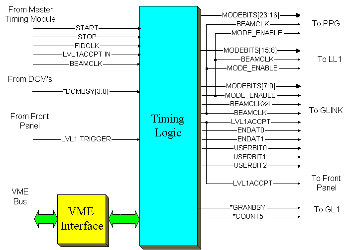
figure 1. Granule Timing Module Block Diagram
The VME interface conforms to the ANSI/VITA 1-1994 VME64 Specification,
and provides additions from the VITA 1.1-199x VME64 Extensions Draft Standard,
Draft 1.4 It is a slave only device.. The board supports A32 Addressing
for all operations, and D32,D16,D08(EO) data transfers. The boards base
address is determined from the geographical address pins GA4-GA0 on the
VME backplane.
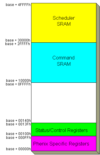
figure 2. Timing Module VME memory map
The first 256 memory locations of the board are reserved for Phenix System Level Registers. Only the first four bytes have been defined, although no values have been assigned as yet, the remaining memory space is reserved for future use.
| BOARD ID: base+0h PHENIX Board ID | |||
|---|---|---|---|
| Field | Bits | R/W | Function |
| TYPE | 31..0 | R | Board Type |
| BOARD NUM | 23..16 | R | Board Number |
| TRANS NUM | 15..8 | R | Transition Modules Attached |
| RSVD | 7..0 | R | Reserved |
table 1. Phenix Defined Registers
The timing subsystem performs three primary functions. First, it is
a mode bit scheduler, which outputs predetermined mode commands on a clock
by clock basis to the FEM's. Second, it provides readout enable strobes
to the FEM's, and monitors the number of level-1-accepts generated by the
level1 system. Third, it provides low jitter distribution and generation
of timing signals, namely the Beam Clock, Beam ClockX4 (generated on board
via PLL), and LVL-1 Accept. Figure 3 below shows the block diagram. Each
of the following functions will be discussed in detail next.
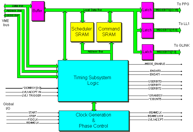
figure 3. Block Diagram of Timing Subsystem
3.1 Mode Bit Scheduler
The Timing Interface provides an eight bit encoded command word (mode bits)
for each beam crossing to all FEM's. Mode commands are defined as
the encoded value of the eight mode bits. Mode commands are grouped
together, into Mode Command groups where a group represents a single
fiducial of the RHIC accelerator. At the current time there are 120 such
beam crossings per fiducial, therefore a Mode Command group consists
of 120 Mode Commands. With the use of an SRAM as the storage devices
for Mode Commands and a separate SRAM containing a list of pointers
(Scheduler Commands) to the beginning of any Mode Command
Group, mode bits can be defined for unlimited number of cycles (with
repetition).
3.11 Scheduler Commands
Scheduler commands are 32 bit instructions loaded in the Scheduler
Memory SRAM, which has a depth of 32K. The scheduler commands
are to be loaded in the order of planned execution. The format for the
scheduler command is shown in table 2. Bit 31 is the retransmit
bit. A logic 1 in this bit will reset the Scheduler, thereby looping back
to the first scheduler command. Using this loopback feature mode
commands may be issued to the FEM's for an unlimited time. Bits 30-8 define
the Scheduler Command repeat bits. The binary value assigned here represents
the number of times to cycle through the current Mode Command Group. Bits
7-0 define which of the 256 unique Mode Command Groups to perform. The
binary value assigned here is a pointer into the Command SRAM to a unique
Mode Command Group. The address of the currently executing Scheduler command
may be read from the Timing Control and Status Registers CYCLE_PTR.
| Field | Bits | R/W | Function |
|---|---|---|---|
| RETRAN | 31 | R/W | Retransmit |
| CYCRPT | 30..8 | R/W | Scheduler Command Repeat Value |
| CYCCMD | 7..0 | R/W | Mode Bit Group Number |
Table 2. Scheduler Command Bit Definitions
3.12 Mode Commands
Mode Commands are 32 bit instructions loaded in the Command
Memory SRAM, which has a depth of 32K. The first byte, (D7-D0) loaded
into this SRAM are the mode bits which are destined to the FEM's via the
GLINK. The next byte, (D15-D8) are for Local Level 1 use and the upper
byte (D23-D16) is for the use of the programmable pulse generator. The
most significant byte, (D31-D24) is reserved for future use. There is room
for storing 256 unique Mode Command Groups (each mode command group consists
of 120, 32 bit, mode commands). The first mode command of each of the mode
command groups must be aligned at 512 byte offsets, as shown below in figure
4.
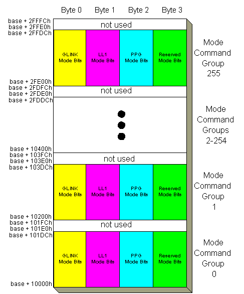
figure 4. Mode Command SRAM
.
3.13 Mode Bit Scheduler Operation
A block diagram of the operation of the mode bit scheduler is shown below in figure 5. A quick overview of the procedure for loading and running the scheduler is described. Mode bits are loaded into the Command SRAM in groupings of 120, which is the number of crossings per fidicial. Each new grouping starts on a 512 byte boundary. Then the scheduling commands are loaded into the scheduler SRAM with the format described in table 3. Up to 32 thousand scheduling commands may be loaded. When the mode bit scheduler starts, by a global start signal, the control logic fetches the first command from the scheduler SRAM and the various fields flow through to the three blocks labeled Cycle Command Base Addr Latch, Repeat Value Counter, and Control Logic. The lower eight bits (CYCCMD) form the upper bits on the Command SRAM, it points to the Base Address of a unique mode bit group. A cycle counter then begins which counts from 0 to 119 on each Beamclk, which provides the lower bits on the Command SRAM. This counter then runs until the Cycle Repeat Field (CYCRPT) has been decremented to zero. The Control logic block recognizes this and then fetches the next command from the scheduler SRAM and the process repeats itself. If the retransmit bit is set (RETRAN), then the next cycle command address will be the first memory location of the scheduler SRAM.
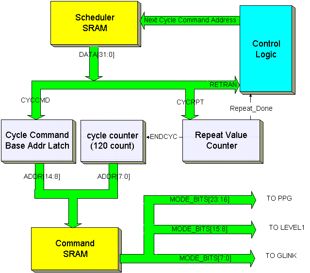
figure 5. Mode Bit Scheduler Operation
3.14 Editing Single and Cycle Commands
To modify and/or read any of the scheduler commands (Scheduler
Memory) and/or mode commands (Command Memory) the module must be in a stopped
mode. Attempting to change this values while the module is in run mode
will have no effect and attempting to read these values while the module
is in run mode will result in undefined data. The control and status registers
are always available to the VME bus.
The procedure for stopping the module is to set the STOP_LOCAL bit of the Timing CSR and then poll on the RUN bit to verify that the module has stopped. (The module may not stop immediately, depending on the value of the bits STOP_EOSF and STOP_EOCC of the Timing CSR) Once the module has been placed in the stopped mode both the scheduler commands and the mode commands may be read and/or modified.
After any modifications have been performed the module may then be restarted either locally or globally by the methods described in the next section
3.15 Global/Local Start/Stop Procedures
The timing module is started and stopped through the global control
inputs: global Start and global Stop. Two control bits, START_ENABLE
and STOP_ENABLE, also exist which enable the modules to accept and
process these Global signals. These control bits allow groups of timing
modules to be synchronously started and stopped. Upon receiving a global
Start pulse and having the control bit START_ENABLE asserted, the
module enters a arming state where it then awaits a Fiducial Clock pulse,
which synchronizes it to a predetermined RHIC accelerator bucket. The next
Beam Clock pulse puts the module into a run mode and mode bits are output.
This is shown in figure 6.
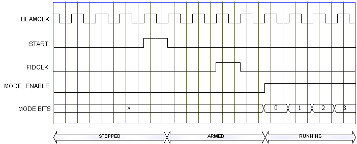
figure 6. Timing Diagram for starting the module
To globally stop the module the board must receive a global Stop pulse and have the control bit STOP_ENABLE asserted. Then depending on the current value of the control bits: STOP_EOSF (stop at end of sequence fifo) and STOP_EOCC (stop at end of current cycle (see section 4.2 for details on these bits)), the module will stop accordingly.
The timing module provides a mechanism for handling the LVL1-Accept
pulses generated by the GL1 System and providing readout enable pulses
to the FEM's based on these pulses.
3.21 LVL1-Accept Handler
To prevent data overrun in the FEM's or in the DCM's, the rate of LV1-Accept triggers must be monitored. This is accomplished by tracking the current number of LVL1-Accepts that are queued for readout with a three bit counter EVT_CNTR. If this counter reaches a value of 5 then a handshake signal *COUNT5 is asserted and returned to GL1, thereby inhibiting it from generating any more LVL1- Accept pulses. Upon assertion of the *COUNT5 signal, a presettable longtime timer, LTTIMER, is started. This timer has a maximum time of about 6.5ms, but may be preset by the user for a shorter duration. When this timer reaches zero, the EVT_CNTR should also be at zero. If it is, the signal *COUNT5 is negated, enabling the GL1 system to resume sending LVL-Accepts. If it is not, then there is a data-flow problem (Most likely the *DCMBUSY input is asserted) and the error bit CNTERR is asserted.
3.22 Readout Enable Generation
With the use of the LVL1-Accept pulses, the Timing Module controls the readout of data from the FEM's to the DCM's with two signals, ENDAT0 and ENDAT1. These two signals are output via the GLINK to the FEM's. In general, when a LVL1-Accept is received the following occurs depending on the current value of EVT_CNTR (described in section 3.21):
LVL1-Accept received when EVT_CNTR = 1
The LVL1-Accept is passed to the FEMs via the GLINK. Also a 16 bit programmable
counter, FEM_CNVRT_TIME is started. This timer allows the front
end to complete the conversion. The nominal time setting for this counter
is 40uS. After this timer has timed out the first data enable (ENDAT0)
is asserted. The width of this signal is the time required for the even
FEMs to transmit their data and is controlled by a 16 bit programmable
counter, ENDAT_TIME. After this timer has timed out, ENDAT0 is negated
and ENDAT1 is asserted. The width of ENDAT1 is the time required for the
odd FEMs to transmit their data and is controlled by the same counter,
ENDAT_TIME. After this timer has timed out, ENDAT1 is negated and
the counter EVT_CNTR is decremented. This is shown below in figure 7.
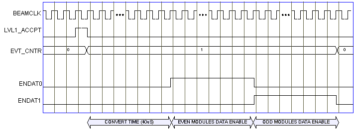
figure 7. Timing Diagram for EVT_CNTR = 1
LVL1-Accept received when EVT_CNTR > 1
The same as the case EVT_CNTR = 1, however the counter, FEM_CNVRT_TIME,
will not be started until the beginning of ENDAT1 has started. This is
shown below in figure 8.
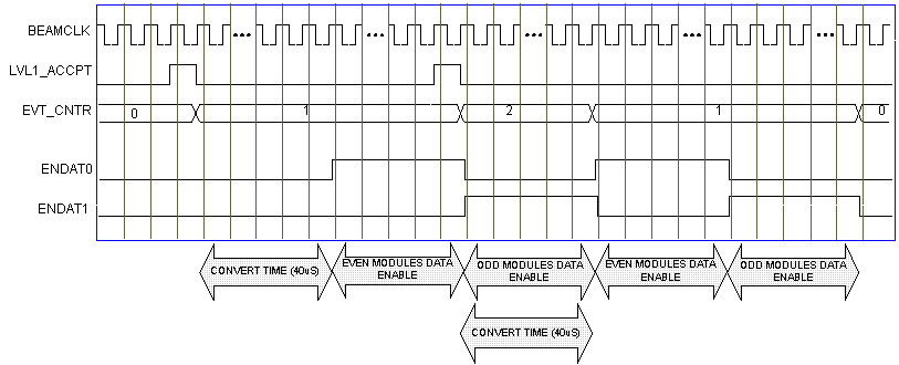
figure 8. Timing Diagram for EVT_CNTR > 1
3.23 Data Collection Module Busy
The input signals *DCMBSY[3:0] is provided from the DCMs, and
is used to prevent the FEMs from passing more data to the DCMs if they
have signalled that they are full, can't unload, etc. This is accomplished
in the logic described above by only letting the current data transmission
(both ENDAT1 and ENDAT2) run to completion. No further LV1-Accepts are
generated by GL1, and when the DCMs are no longer "busy", the
above protocol resumes. The four *DCMBSY signals are internally or'd together
to produce the signal *GRANBSY which is passed back to the global level
1 system.
3.31 On Board Clock Generation
The BeamClkX4 is generated on board via a programmable skew clock buffer. The Cypress part CY7B991 provides a low jitter output (<25ps RMS) for the BeamClkX4. The part multiplies the BeamClk by a factor of four which directly drives the clock input to the GLINK.
3.31 Phase Delay
The incoming BeamClk signal can be delayed between 10ns - 132ns
via on board programmable delay generators. The resolution of this delay
is +/- 20ps. There are three registers for controlling the phase delay
of the BeamClk Signal. FINEDLYADJ controls an MC10E195 programmable
delay chip whose typical range is 1.39ns - 3.63ns over 128 steps. COURSEDLYADJ
controls a DS1020 programmable delay chip whose typical range is 10ns
- 48.25ns over 255 steps. Finally, ROUGHDLYADJ simply delays the
BeamClk signal by delaying it by single 37Mhz periods giving discrete delays
of 0,27ns,54ns,and 81ns. By combining these three delay methods a continuous
range of delay can be programmed for the BeamClk. See section 3.3 for details
on the register values.
All outputs from the Timing Interface will be placed onto a Hewlett
Packard HDMP-1012 Transmitter (GLINK). This virtual ribbon cable interface
provides a high speed serial path for 20 parallel bits. The bit assignment
for the timing signals is shown below in table 3
.
| Data Line | Function |
|---|---|
| D0 | Mode Bit 0 |
| D1 | Mode Bit 1 |
| D2 | Mode Bit 2 |
| D3 | Mode Bit 3 |
| D4 | Mode Bit 4 |
| D5 | Mode Bit 5 |
| D6 | Mode Bit 6 |
| D7 | Mode Bit 7 |
| D8 | Beam Clock (9.4Mhz) |
| D9 | LVL1 Accept |
| D10 | Mode Enable |
| D11 | EnDat0 |
| D12 | EnDat1 |
| D13 | User Bit 0 |
| D14 | User Bit 1 |
| D15 | User Bit 2 |
| D16 | Reserved |
| D17 | Reserved |
| D18 | Reserved |
| D19 | Reserved |
Table 3. GLINK Bit Assignments
The GLINK will be clocked at four times the Beam Clock (BeamClkX4) which has been generated via an on board PLL and will have a maximum jitter of 25ps rms. All other signals will have a frequency no greater than the BeamClk. The BeamClk signal (D8) will always be present and will provide phasing information for the BeamClkX4 signal. The BeamClkX4 should be used as the accurate timing reference, and the BeamClk signal used to indicate the beam crossing (zero to one transition on BeamClk).
The Three User Bits are levels which are mapped directly from VME space. Their encoded value represents various functions for FEM's to perform. Refer to section 3.4 for the definition of these values
The following section provides specific information on programming and
controlling the timing subsystem through its control & status registers
via the VME interface.
| TIMING CSR: base+100h Mode Bit Scheduler: Control & Status | |||
|---|---|---|---|
| Field | Bits | R/W | Function |
| CYC_RETRAN | 0 | W | Asserting this bit resets the scheduler SRAM pointer to the first scheduler command. This pointer value may be read from the SCHEDULER_PTR Register. |
| STOP_EOSF | 1 | R/W | When this bit is asserted to a logic 1, the cycle commands will stop executing as soon as a scheduler command with the retransmit bit asserted is completed. When at logic zero, the scheduler commands will repeat indefinitely. |
| STOP_EOCC | 2 | R/W | When this bit is asserted to a logic 1, the cycle commands will stop executing as soon as the current scheduler command is completed. |
| START_ENABLE | 3 | R/W | Asserting this bit high will enable the module to process a Global Start signal. If it is at logic zero, the module will ignore any Global Start signals. Resets to logic zero. |
| STOP_ENABLE | 4 | R/W | Asserting this bit high will enable the module to process a Global Stop signal. If it is at logic zero, the module will ignore any Global Stop signals. Resets to logic zero. |
| RUN | 5 | R | A logic 1 indicates that the module is currently sending valid mode bit commands. A logic 0 indicates the module is stopped. |
| WAIT | 6 | R | A logic 1 indicates that the module has received a global start pulse, and is awaiting a global fiducial clk pulse to enter the run state. |
| TIMING CSR: base+104h Mode Bit Scheduler: Cycle Pointer | |||
|---|---|---|---|
| Field | Bits | R/W | Function |
| SCHEDULER_PTR | 15..0 | R | This value is the memory address of the current cycle command being executed in the Scheduler Memory. |
| TIMING CSR: base+108h Mode Bit Scheduler: Command Pointer | |||
|---|---|---|---|
| Field | Bits | R/W | Function |
| COMMAND_PTR | 15..0 | R | This value is the memory address of the current command being executed
in the Command Memory. |
| TIMING CSR: base+10Ch LVL1-Accept & Read Out Enable: Control & Status | |||
|---|---|---|---|
| Field | Bits | R/W | Function |
| COUNT5 | 0 | R | This is the current value of the global output *COUNT5 that
goes to GL1 (see section 3.21) 0=COUNT5 negated, 1=COUNT5 asserted |
| DCMBUSY[3:0] | 4..1 | R | This is the current value of the global inputs *DCMBUSY that
comes from the Data Collection Modules (see section 3.23) 0=DCMBUSY negated, 1=DCMBUSY asserted |
| GRANBUSY | 5 | R | This is the grand-or of the four DCMBUSY registers 0=GRANBUSY negated, 1=GRANBUSY asserted |
| CNTERR | 6 | R/W | This bit is asserted if the timer, LTTIMER, has timed out and EVT_CNTR is not equal to zero. Indicates a data-flow problem. This bit may be cleared (see section 3.21) |
| TIMING CSR: base+110h LVL1-Accept & Read Out Enable: Event Counter | |||
|---|---|---|---|
| Field | Bits | R/W | Function |
| EVT_CNTR | 2..0 | R | Current Number of LVL1-Accepts events currently being processed. |
| TIMING CSR: base+114h LVL1-Accept & Read Out Enable: LongTime Timer | |||
|---|---|---|---|
| Field | Bits | R/W | Function |
| LTTIMER | 15..0 | R/W | Preload value of the LongTime Timer (see section 3.21) LTTIMER = Timer Length / 108ns |
| TIMING CSR: base+118h LVL1-Accept & Read Out Enable: FEM Convert Timer | |||
|---|---|---|---|
| Field | Bits | R/W | Function |
| FEM_CNVRT_TIME | 15..0 | R/W | Preload value of the FEM Convert Timer (see section 3.21) FEM_CNVRT_TIME = Timer Length / 108ns (initialized to 40us (172h)) |
| TIMING CSR: base+11Ch LVL1-Accept & Read Out Enable: Enable Data Timer | |||
|---|---|---|---|
| Field | Bits | R/W | Function |
| ENDAT_TIME | 15..0 | R/W | Preload value of the Enable Data Timer (see section 3.21) ENDAT_TIME = Timer Length / 108ns (initialized to 40us (172h)) |
| TIMING CSR: base+120h Clock Generation & Phase Control: Fine Delay Control | |||
|---|---|---|---|
| Field | Bits | R/W | Function |
| FINEDLYADJ | 6..0 | R/W | Fine Adjust of Phase Delay for the BeamClk. Range is approx 0 to 2ns.
Corresponds to the bits on the MC10H195 |
| TIMING CSR: base+124h Clock Generation & Phase Control: Course Delay Control | |||
|---|---|---|---|
| Field | Bits | R/W | Function |
| COURSEDLYADJ | 7..0 | R/W | Course Adjust of Phase Delay for the BeamClk. Range is approx 0 to
48ns. Corresponds to the bits on the DS1020 |
| TIMING CSR: base+128h Clock Generation & Phase Control: Very Course Delay Control | |||
|---|---|---|---|
| Field | Bits | R/W | Function |
| ROUGHDLYADJ | 1..0 | R/W | Very Course Adjust of Phase Delay for the BeamClk. Uses the 37Mhz clock to delay the beamclk in 27ns step intervals. 00=0ns, 01=27ns, 10=54ns, 11=81ns. |
| TIMING CSR: base+12Ch GLINK Interface: User Bits | |||
|---|---|---|---|
| Field | Bits | R/W | Function |
| USER_BITS | 2..0 | R/W | Sets the level of the GLINK bits D13 (Bit 0),D14(Bit 1),D15 (Bit 2) These bits are encoded to represent the following functions: 000 : no function |
| TIMING CSR: base+130h GLINK Interface: Reset GLINK Transmitters | |||
|---|---|---|---|
| Field | Bits | R/W | Function |
| GLINKRESET | 3..0 | R/W | Resets the selected GLINK transmitter. Selected GLINK is encoded into the four bits. A write value of Fh has no effect. When reset of the GLINK reset has completed a value Fh will appear as readback. |
| TIMING CSR: base+134h Reserved | |||
|---|---|---|---|
| Field | Bits | R/W | Function |
| RSVD | 15..0 | R/W | This register has been reserved for future use |
| TIMING CSR: base+138h Reserved | |||
|---|---|---|---|
| Field | Bits | R/W | Function |
| RSVD | 15..0 | R/W | This register has been reserved for future use |
| TIMING CSR: base+13Ch Reserved | |||
|---|---|---|---|
| Field | Bits | R/W | Function |
| RSVD | 15..0 | R/W | This register has been reserved for future use |