|
|
|
| Previous slide
| Up to slide index
| Next slide
| |
|
|
|
| Previous slide
| Up to slide index
| Next slide
| |
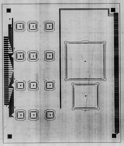
A picture of the substrate layout is at the bottom of this page. (there were actually several overlays showing the interconnections, but I don't know how to do that in HTML)
The substrate is 48x40 mm rectangular and 1.52 mm thick, fired, white alumina (Al2O3, 96%. It has 14 milled wells for 12 custom Asic chips and 2 Xilinx chips.
Components:
I/O Contacts:
Circuitry:
General Information:
This is a 5x enlarged scale model of the 32-channel prototype of the MVD FEE. The final implementation will service 256 channels. It is an MCM (Multi Chip Module), where bare die, or unpackaged chips, are mounted in wells in a ceramic substrate, with their contacts facing up. A layer of polyamide, a kapton-like material, is mounted over the top. A laser drills vias, or holes, through the polyamide to some of the contact points. Then a layer of metal contact lines is laid down by photolithographic means, and the next layer of polyamide is applied. The process is repeated 4 times. Finally, some external components are mounted onto the assembly.