- Schematic procedure for calibration runs. (MJL 12/1/00).
- Control of the calibration system via ArcNet in the counting house. (MJL 10/30/00).
- Notes on running the muTr DAQ in word and
in postscript . (MJL 12/1/00).
- User notes on control of the calibration system via ArcNet in 905 on the PC. (MJL 9/13/00).
- Changing the ArcNet daughter card on the calibration ArcNet board. (MJL 3/4/02).
- Operation Notes for the VME Calibration boards (MJL updated 6/26/00).
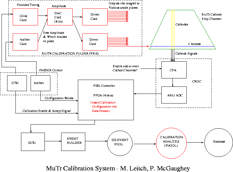
- Top level diagram in postscript or gif
of MuTr Calibration Syste (MJL & PLM 3/1/00).
- Summary of the muTr Calibration System (MJL & PLM 1/14/00).
- Specification of bits for calibration tagging of data by FPGA (MJL 3/1/00).
- Configuration of the calibration pulser system via ArcNet and
the LabView program source code in V5.1
or V5.0 for configuration via the parallel port (PLM 3/6/00).
- Note on the Anode Pulsing Method of Calibration in postscript
or word (DML & MLB).
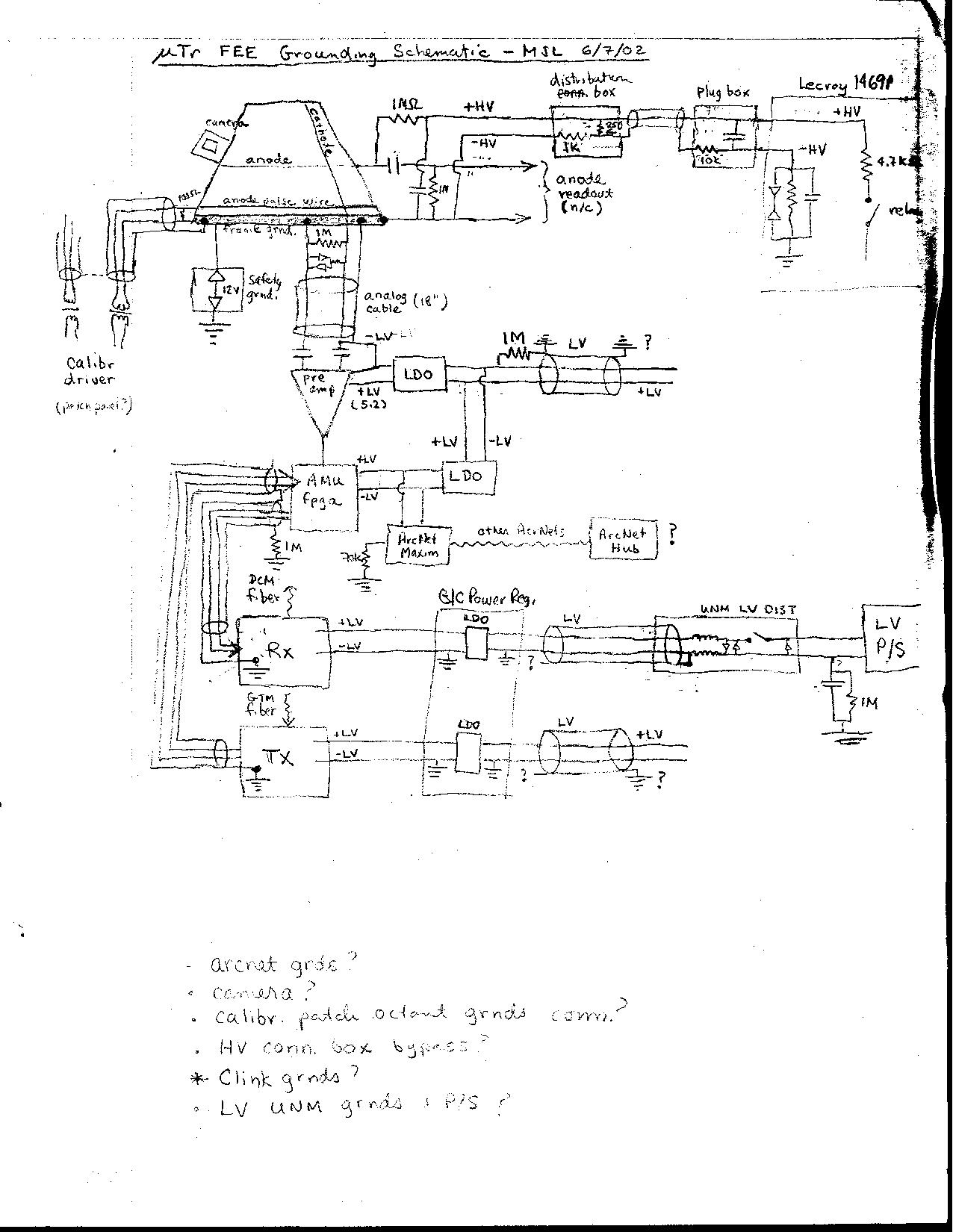
- Overall Schematic of the muTr Calibration System (MJL & PLM 1/20/00).
Production versions of calibration boards:
- Driver board layout (gzipped postscript) or (pdf),
pcb file (ExpressPCB file)
and parts list (text) (ad8016o, 7/6/00).
- DAC board layout (gzipped postscript) or (pdf),
pcb file (ExpressPCB file)
and parts list (text) (daqn, 7/12/00).
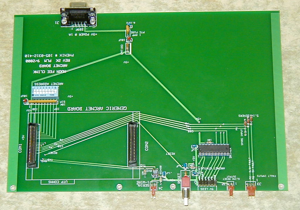
- ArcNet board layout (gzipped postscript) or (pdf),
pcb file (ExpressPCB file)
and parts list (text) (arcnetj, 7/12/00).
- Glink board layout (gzipped postscript) or (pdf),
pcb file (ExpressPCB file)
and parts list (text) (fiberl, 7/12/00).
- Layouts for the stations 1 and 2; and for station 3 calibration patch panels.
Production versions of boards for the Glink/Clink crates:
- Glink/Clink LV regulators - 2004 version.
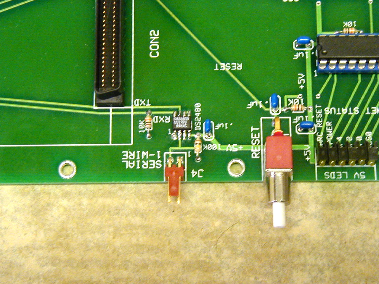
- Glink/Clink crate ArcNet board layout (gzipped postscript)
or (pdf),
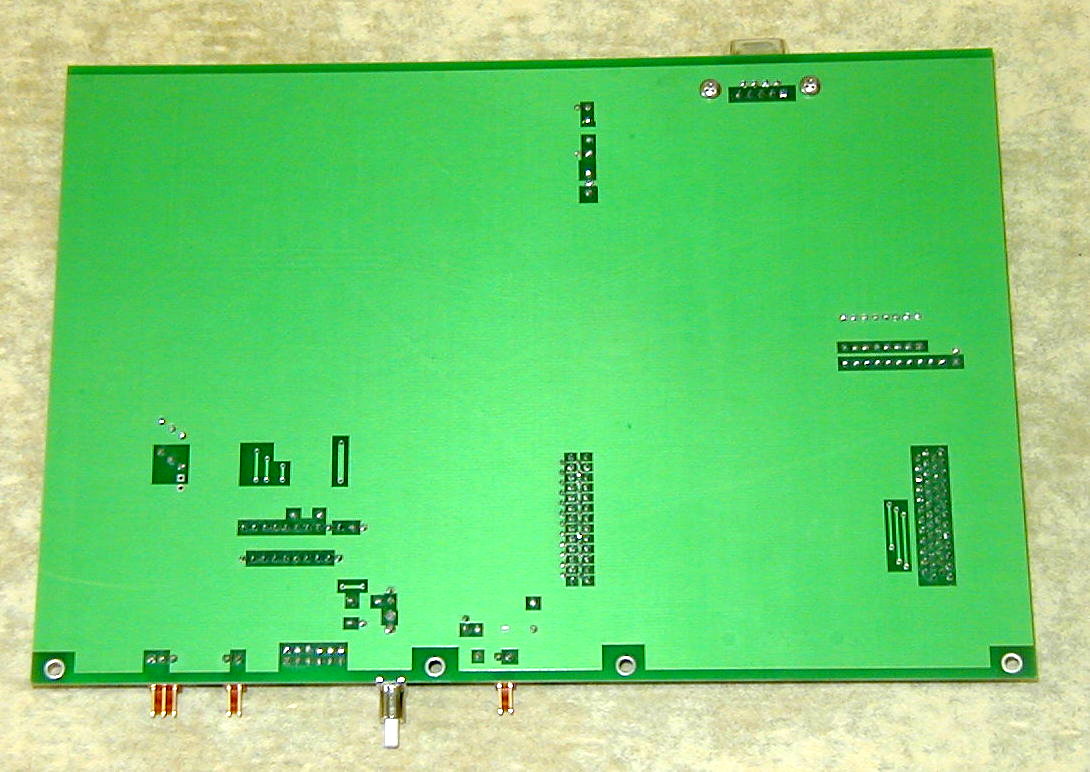
digital pictures of the front and back of the board,
and a closeup,
pcb file (ExpressPCB file)
and parts list (text) (farcnetk, 10/10/00).
- Glink/Clink crate power regulator board layout (gzipped postscript)
or (pdf),
pcb file (ExpressPCB file)
and parts list (text) (fpowerk, 10/10/00).
- Physical layout for the DAC, Driver
ArcNet and GLink boards.
- Schematics of the DAC board, pages 1, 2,
3, 4, 5,
6, 7.
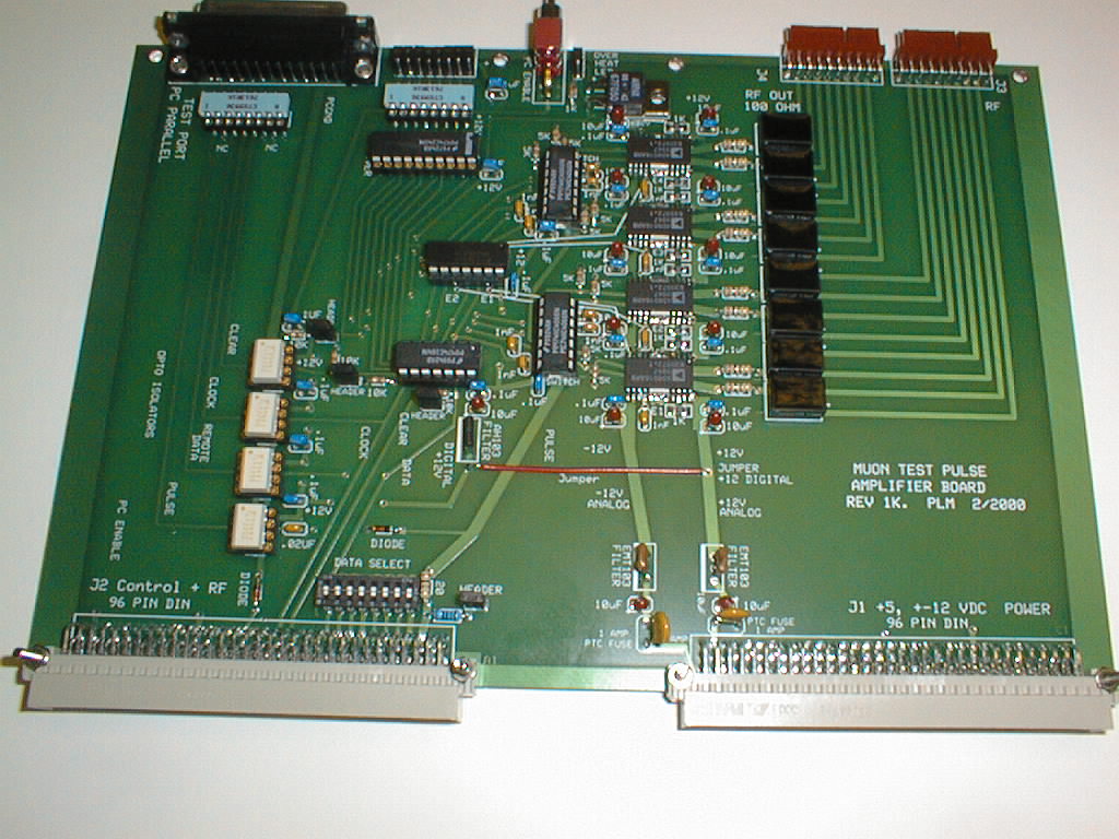
- Schematics of the Driver board, pages 1, 2,
3, 4, 5,
6, 7, 8.
- Schematics of the ArcNet board, pages 1, 2,
3, 4, 5.
- Schematics of the Glink board, pages 1, 2,
3.
- Picture of Driver board.
- Specs of wire used for calibration system to take signals into chambers.
- Specs for round Ampenol page1 and page2
and Molex connectors used for calibration system cables which take signals into chambers.
- Pinout for the long calibration cable connectors.
- Pinout and Length for the short calibration patch cables.
- Pigtail description and connections.
- Description of how to test pigtails with the calibration system in bldg. 905.
- Charge output (using function approximating preamp on pulse
as recorded on digital scope trace) versus DAC. Assuming a 0.25% error on each measurement
and has a chi2/ndf of less than one. Thus we are well under our design goal of 1% and
can use a linear response function, even at large pulse height (PLM/MJL 9/11/00).
- Voltage versus time as output from a calibration driver board into 100 ohms (MJL 10/1/00).
- ADC counts for 4 samples vrs strip # for DAC = 0x00, 0x19,
0x32, 0x64 and 0xff (MJL 6/27/00).
- ADC rms for 4 samples vrs strip # for DAC = 0x00, 0x19,
0x32, 0x64 and 0xff (MJL 6/27/00).
- ADC counts vrs time from calibration system for channels 1-8
and 17-24 when calibration DAC level set to 64 (MJL 4/1/00).
Some other related items (but not part of calibration system):
- Schematic of the Glink/Clink ArcNet system including cable lengths and arcnet addresses.
- Documentation for the Glink/Clink power regulator and ArcNet cards.
- Safety Committee Minutes (word file) for review of PHENIX Low-voltage power supplies and Racks.
- Layouts of the Glink/Clink power regulator,
Arcnet power and Dallas chip interface
and CROC test pulse interface boards.
- Schematics of the Glink/Clink power regulator,
Arcnet power and Dallas chip interface sheet 1,
2, 3
and 4,
and CROC test pulse interface boards.
- Schematic of 12 volt diode protection box.